ENGR338 Lab 2022
Fall
Lab 3 Layout R-2R Ladder DAC
Name: Mason
Brady
Email:
mrbrady1@fortlewis.edu
Layout of an R-2R DAC
Introduction:
This lab uses a Electric VLSI to layout 10k resistors to create a DAC.
A subcell is created containing a 1-bit DAC which can then be compied
and placed in series to create larger DACs.
Materials:
LTSpice, Electric VLSI
Methods:
The first task was simple, create a subcell of a 1-bit DAC. This used 3
10k resistors, 2 in series and one in parallel which is connected to an
off page connector. An offpage connector is connected to the 2
resistors in series as well and a final off page connector was placed
at the branch point. An icon of the subcell was then created, all of
which can be seen below in Figure 1.
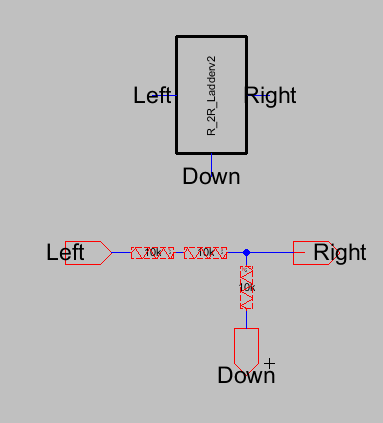
Figure 1.
1-bit DAC subcell.
10 of these were then placed in series with a 10k resistor at the
bottom to create the following DAC:
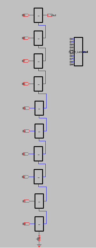
Figure 2. 10-bit DAC
schematic.
A layout was then created for the subcell using a width of 15 and
length of 187.5 for a resistance of 10k. These were placed 25 apart.
These were all then connected to eachother and the top resistor goes to
the left output, the middle resistor to the right output, and the
bottom to bottom. This was then packaged and placed in series with 9
more identical cells as done with the icons which created the schematic
seen in Figure 3.
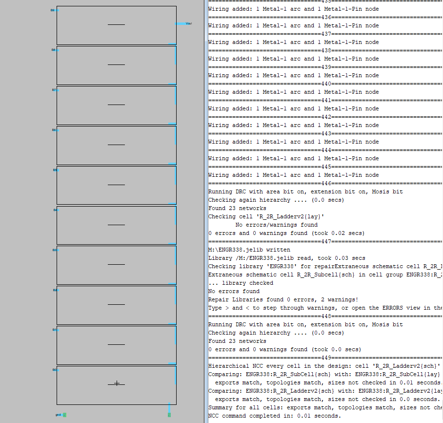
Figure 3. Layout
of 10-bit DAC.
The whole layout was DRC and NCC clean as seen in the figure.
Results:
The aformentioned shcematic was placed with an ideal ADC like the prior
labs and run in LTSpice as seen below in Figure 4.
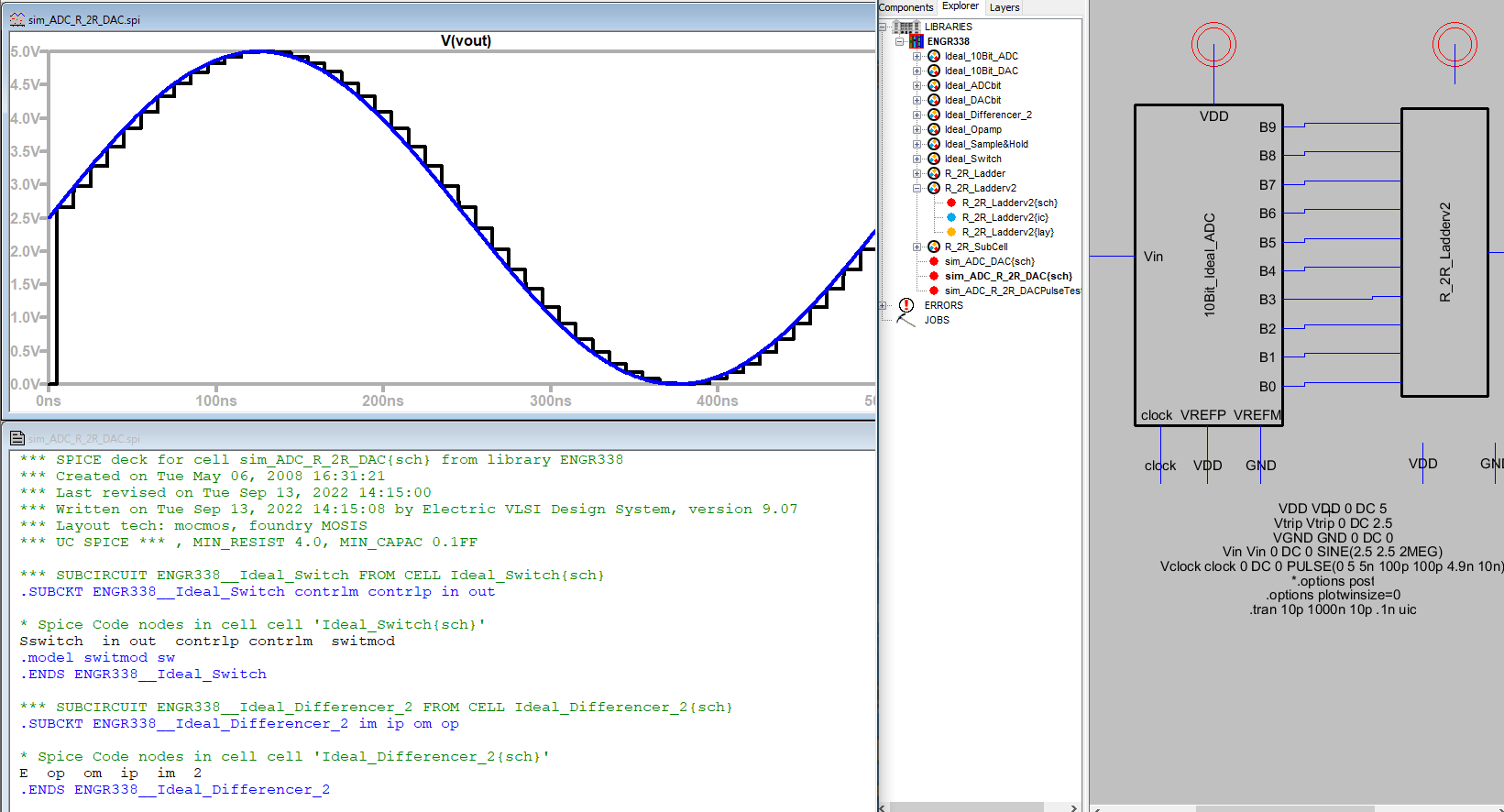
Figure 4. Simulation results from ideal ADC and R_2R ladder DAC
confirming the DAC works as intended. Some of the wiring was
graphically missing but connected properly.
Discussion: This
lab was interesting and it was cool to see how the n-well resistors get
placed on a chip and that they actually work.